by Chris DePuy, 650 Group / November 4, 2026.
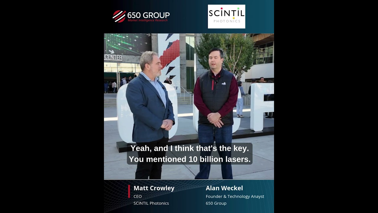
At the 2026 OCP Global Summit, SCINTIL Photonics pitched its laser-integration process. CEO Matt Crowley made the company’s case to Alan Weckel, Founder and Technology Analyst at 650 Group. 650 Group filmed the exchange and published it on its YouTube channel, the first two parts of a three-part series. The summit drew 15,000 attendees from October 12 to 15, 2026. That is a 38 percent increase over 2025, per the event page. The weight for the data center network market sits in Crowley’s manufacturing constraint: the optical interconnect, not the accelerator.
Where is the real bottleneck in the AI data center build-out?
If you buy optics, the port-growth quote is the one to act on. If you build the components, the wafer math is the one to plan around. It depends on which side of the transaction you sit on. Crowley’s framing in Part 2 starts from a scaling identity. As he says: “As the number of XPUs grows, the number of ports is growing.” The stated conclusion follows: “the network is becoming more of a bottleneck on the manufacturing side than the XPUs themselves.”
The consequence is commercial, not technical: “if I can’t get the interconnect onto my chips, I can’t get data on and off, and I basically can’t sell the chips.” That is a supplier telling an operator market one thing, as of November 2026. Optics fab capacity is the queue in front of the accelerator queue. The same port pressure shows up at desk scale. These pages profiled four DGX Sparks carrying NVIDIA’s official NVFP4 checkpoints earlier this autumn.
The SCINTIL Photonics SHIP process bonds III-V lasers onto silicon wafers
The company’s answer, described in Part 1, targets what silicon photonics left unsolved in the bill of materials. Crowley’s starting observation is that the platform “has been a huge advancement and a huge successful technology.” The follow-on: “the lasers and amplifiers and all these things, they’re still left off chip. I still have to glue those on. I still have to solder them.” SCINTIL Photonics describes SHIP, its heterogeneous integration process, on its own about page as a silicon-plus-III-V photonic platform. The about page: “through a unique die-to-wafer bonding of III-V material on silicon,” in mass production on commercial semiconductor foundries.
The technology is more than fifteen years old. CEA-Leti in France developed it before SCINTIL commercialized it, per the company’s about page. The company holds its headquarters in France, runs fabless, and maintains Canadian and US offices. Crowley states the effect plainly: “We basically take lasers and turn them from a discrete component into an element that’s on a bigger chip.” What SCINTIL sells, in his words, are multi-wavelength laser sources. In-house design work covers lasers, amplifiers and modulators.
How SCINTIL Photonics gets to ten billion lasers
The demand number Crowley anchors the pitch to is the laser count the AI data center build-out implies. His critique is of who is trying to make them. Later in the interview he argues “the telecom industry traditionally was a low-volume, somewhat craft manufacturing industry.” “They were never built to build 10 billion lasers,” he continues. His remedy is to run the active devices through semiconductor manufacturing practice: doing the math, “if I’m making the SCINTIL process on a 200 and soon to be 300 millimeter wafer, I’m going to be getting 10,000 lasers on a single wafer,” on standard silicon photonics lines rather than specialty fabs.
The foundry base for that claim is not hypothetical. SCINTIL’s own news post documents its III-V distributed-feedback lasers and amplifiers integrated on Tower Semiconductor’s production silicon photonics process. The foundries already know the scaling question, Crowley notes in the interview: “They’re used to scaling.” The arithmetic he offers next is the one worth holding onto: “The number of wafers you need to build 10 or 20 billion lasers is tiny compared to the number of CMOS wafers in manufacture.” Put multiple wavelengths on every port, he adds, and “you actually get to these billions of wavelengths pretty quickly.”
Why the SCINTIL Photonics wafer math outlasts the demand quote
Three things in this exchange deserve the reader’s attention as of November 2026. First, Crowley states demand without hedging on the supplier side. Part 2 opens on the manufacturing theme: “we basically see almost unlimited demand for lasers and for optical networking.” Second, Crowley makes the reliability-and-cost argument on wafer economics rather than on link budgets or transceiver specs. Wafer economics is the currency semiconductor manufacturers actually manage. Third, the bottleneck claim inverts the usual order of AI infrastructure anxiety. The accelerator gets the headlines, and the optics fab sets the shipping date. I read the wafer arithmetic, not the demand quote, as the durable claim SCINTIL Photonics makes in these interviews. Anyone sizing the optical component market should ask how many lasers fit on a 300 millimeter wafer first. How many XPUs a rack holds comes second.
This migration of lasers and amplifiers onto silicon photonics process lines touches every layer of the scale-up network stack. Firms such as 650 Group have been tracking it in their AI infrastructure research. The manufacturing capacity behind the optical component market is the variable to watch as clusters outgrow the electrical interconnect.